avialable in the groups of apl.Prof. Wendler & Prof. Ronning
beam line
Ion beams
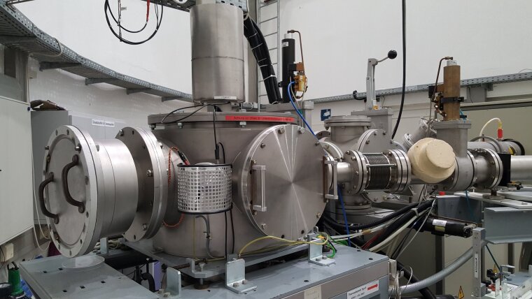
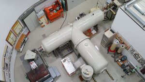
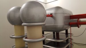
Tandem accelerator "JULIA"
3 MeVTandetron accelerator JULIA equipped with a sputter ion source and a duoplasmatron, as well as with an universal beam line for ion implantation and ion beam analysis (IBA). Possible ion beam energies are from 500 keV to 12 MeV, and traget temperatures can range from 15 K to 1500 K. Aviable ion beam analysis techniques are RBS, Channeling, NRA, PIXE, and PIGE.
Ion accelerator "ROMEO"
Ion implanter ROMEO, which can be used for ion implantation of basically any element with ion energies in the range from 10 keV to 400 keV. te target can be cooled down to 15 K and heated up to 1500 K. sample areas are limited to some mm2 up to 2 inch wafer. Three dimensional nanostructurescan be rotated and implanted under an angle of 45 Grad.
Ion implanter LEILA for low ion energies in the range from 0.5 keV to 10 keV. Can be used for hydrogen passivation of surfaces and the ripple formation by nobel gas ions.
One FEI dual beam FIB with high-resolution electron and Ga ion beams. Deposition of Pt, Au, SiO2, and XeF2 etching. Micro manipulator. Automated preparation of TEM-Lamellen and chracterization with STEM at 30kV. Ion beam / electron beam induced current (IBIC/EBIC).
One Ion beam deposition systemMr. Stringer equipped with an 30 keV ion beam, mass separation, electrostatic de- and acceleration unit. Ideal for the synthesis of diamond-like materials. Furthermore, this system can be used for ion implantations in the ion energy range from 100 eV to 60 keV.
Structural characterization of solids
One JEOL scanning electron microscope (SEM) with energiy disperse X-ray spectroskopy (EDS) for element analysis. Equipped with an LaB6-Cathode and thus a resolution of minimal 5 nm.
One FEI dual beam FIB mit high-resolution electron micrsocope (resolution < 1 nm) und Ionensäule. Deposition of Pt, Au, SiO2, and XeF2 etching. Micro manipulator. Automated preparation of TEM-Lamellen and chracterization with STEM at 30kV with a resolution of about 1 nm.
Access to a JEOL JEM-3010 transimission electronen microskope (TEM) with energiy disperse X-ray spectroskopy (EDS) for element analysis. Equipped with an LaB6-Cathode an a maximal resolution of 0.17 nm. This is in equipment belongs to the group of Prof. Rettenmayr.
Access to several X-ray diffraction systems (XRD) at IOQ.
X-ray absorption spectroscopy (XAS, EXAFS, XANES) at different ssynchrotron systems, e.g. DESY, ESRF or SLS. Furthermore lateral resolved X-ray fluorescence analysis (XRf), X-ray diffraction (XRD), X-ray absorption spectroscopy (XAS) and X-ray induced current (XBIC) with a synchrotron nano beam at ESRF.
3 MeV Tandetron accelerator JULIA for ion beam analysis (IBA) such as RBS, Channeling, NRA, PIXE and PIGE.
Electrical characterization of solids
Photo lithography in a clean room for the preparation of contacts & bonder.
automated systems for voltage-current characteristics (IV): - down to pA (4-point measurement) - at room temperatur with AM 1.5 solar seimulator or in dark - from 10 K to 500 K under illumination with diffrenet wave lengths
Capacity voltage measurements (CV) form 10 to 500 K in order to determine doping profiles.
Thermal admittance spectroscopy (TAS) for the investigation of shallow and deep dopants.
Temperature dependent capacity transient spectroscopy (DLTS) for the determination of the carrier concentration and activation energy of deep impurities.
Hall effect system (80 K - RT) for the determination of the carrier concentration and activation energy of dpoants.
Optical characterization of solids
Micro photoluminescence (PL) spectroscopy: 500 mm gratting monochromator, UV-VIS CCD (200 - 1100 nm), iCCD (200 - 850 nm), InGaAs-Array (800 - 1650 nm), temperature range 4-300 K, time resolution of 3 ns, spatial resolution ~1 µm, laser sources: HeCd (325 nm cw), Nd:YAG (7 ns Pulse, 266, 355, 532 nm, 1-200 Hz), NeNe Laser (633 nm cw), PL excitation spectroscopy (PLE) using a Xe lamp with a 200 mm Monochromator (250-1100 nm).
One SEM (JEOL) isequipped with cathodoluminescence (CL) for the analysis of the optical properties of semiconductor nanostructures. It consists out of a 300 mm monochromator and two photomultipliers for the visable (250-900 nm) and infrared range (300 - 1650 nm). CCD Kamera (200 - 1100 nm) for the fast acquisition of spectra. Cryo stage for sample temperaturesfrom 6K to 300 K. (funded by EFRE)
Varian UV-VIS spectrometer (185-3300 nm) for the measurement of absorptions, transission or reflexion spectra. Ulbricht sphere for direct and diffusive scattering.
Varian FTIR spektrometer (400-6000 cm-1) fof the measurement of IR Spektra in absorptions, transmission, or reflection geometry.
Thin film synthesis
Sputter deposition system for the synthesis of metallic films (Cu, In, Ga)
Sputter deposition system for the deposition of TCO front contacts (transparent conducting oxides)
Suptter deposition system for the deposition of Mo back contacts
Synthesis of semiconductor nanowires and processing
CVD system for the synthesis of semicondctor nanowires. Consiting out of a three zone furnace with a maximum temperature of 1350 °C, one roughing pumpe (10-3 mbar), two gas flow controllers, and a cooling system. Full computer driven.
High temperature furnace for the synthesis of semicondctor nanowires at a maximum temperature of 1500 °C, one roughing pumpe (10-3 mbar), two gas flow controllers, and a cooling system. Full computer driven.
Tube furnace with gas Flow (air, oxygen, nitrogen, argon) for the growth of nanostructure and annealing of samples.
Serveal (high temperature) furnaces for annealing up to 2050 K under vacuum or inert / reactive gases, e.g. for the activation of thin films.
One system for rapid thermal annealing (RTA) .
One FEI dual beam FIB with the local depotion of Pt, Au, SiO2, or. XeF2 etching.
Photo lithography in a clean room for the preparation of contacts & bonder.